
Product
Product features
- Meets AEC Q100, Grade 0 criteria
- Fully CMOS process compatible
- No impact on the existing devices and SPICE model
- All IP assets can be reused because the same PDK is applied
- Low cost
- 0 ~ few additional masks
- Short testing time


Technology
The Advantage of SONOS
Floadia’s G1 and G2 are based on SONOS memory architecture, which has many advantages over widely used Split Gate memory architecture.
High Reliability
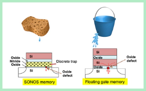
The mechanism of Electric charge retention with distributed charge trap applied to SONOS type, is different from the other ones such as Floating Gate Charge storage type.
SONOS is free from leakage of electric charge through defect or weak spots in the Bottom Oxide film caused by damage during Program and Erase operation, because trapped charges are tightly bonded with the trap site in Silicon Nitride Film.
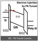
Floadia’s SONOS technology employs Fowler Nordheim (FN) tunneling mechanism for the Program and Erase operation.
The current level of FN tunneling is in the order of pA/cell, and the Oxide damage caused by electric current through the film during Programing which limits the endurance life is negligibly small.
High reliability – Stable Vt
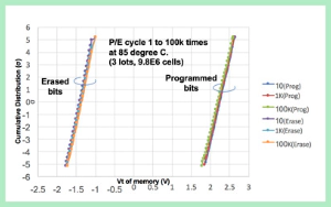
Vt distribution of memory cell is very narrow and stable without multiple cycles of verification and re-programming. Even after 100 thousand cycles of program and erase are executed, no deterioration is observed nor outlier bit.
In addition, electrons and holes are injected uniformly in the whole channel area. This behavior also works positively to maintain oxide quality high.
Easy to Manufacture
Floadia’s SONOS memory cell consists of the most commonly used materials, so it is easy to implement into foundry’s existing manufacturing process flow.
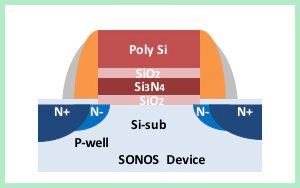
PolySi/SiO2/Si3N4/SiO2/Si (SONOS)
FN tunneling is the best match for Charge Trap System because, electric field can be weakened with charge (electron/hole) trapped in SiN film even with manufacturing defects. Also, when tunneling the whole channel area, electrons and holes are injected evenly to make electric field uniform.
Large Programming Size enables Short Testing Time
Floadia’s SONOS memory is using FN tunneling technology to achieve extremely low power in program and erase.
It consumes 1/1,000,000 times current, compare toconventional technologies using hot carrier injection for program/erase operation.
This also helps reducing testing time, which dominates large portion of the chip cost.
In addition, electrons and holes are injected uniformly in the whole channel area. This behavior also works positively to maintain oxide quality high.
High Speed Non Volatile SRAM
Floadia’s G2 offers very unique feature supporting “read operation” with VDD. This is only available from Floadia. Conventional eNVMs usually require high or mid-high voltage during Program/Erase/Read operation. High voltage supply for G2 cell is only required to Memory Gate, and the power supply unit is normally placed in outside of the memory block. Because of elimination of high voltage area in the memory block, memory cells and logic circuits are allowed to connect directly without having isolation area. When G2 cells and SRAM cell are directly connected, this new type connected cell works as Non-Volatile SRAM. Floadia will provide more new applications utilizing unique feature of G2.
Marriage of Logic and Flash
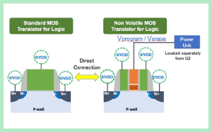
G2 cell consists of one SONOS transistor and two switching transistors placed adjacent to SONOS transistor. This tri-gate transistor works as one Non-Volatile transistor operated by logic level voltage to switching transistors and high voltage only to SONOS memory gate. Because of quite low programing current, pA order to each cell which is equivalent 1/1,000,000 of Floating Gate NVM, the wiring to SONOS memory gate is treated like a signal line. And power supply unit is allowed to place outside of memory block such as a corner area of the die. This unique feature of G2 provide LSI designers freelines of chip design and creation of new circuits combining logic circuits with Non-Volatile functionality.
Non Volatile SRAM
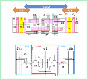
High Speed Non-Volatile Random-Access Memory (NV-SRAM) is the one of dream device which may impact dramatically change on architectural design of MCU, SOC and FPGA. Floadia offers new and very practical solution to make NV-SRAM combining two G2 cells with six transistor SRAM cell directly. RAM functionality is realized by SRAM portion of NV-SRAM as usual SRAM operation, and the data stored in SRAM will be transferred to G2 cell when shutting/power down, also the data stored in G2 cell will be transferred to SRAM when power on. This new NV-SRAM offers high speed NV-SRAM functionality without using any new materials in very simple way.
MCU with NV-SRAM
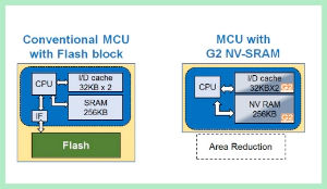
High Speed NV-SRAM can change memory architecture of MCUs and provides great advantages, such as elimination of dedicated Flash block and Inter Face circuit, as well as excess loading time from and to Flash block. Utilizing this new architecture, the MCU system will have sleep mode in very fine granularity or quick start.